
Design | PCB Design, Circuit Design, Autodesk Revit, Fusion 360
Complete Eagle CAD PCB Design

WHY THIS COURSE?
Strong hold in basic electronics.
Circuit Design capability.
Circuit analysis & ERC.
Components knowledge.
Power Supply designing.
Power Integrity Analysis.
Multiple PCB-CAD tool expertise.
Expert in library creation.
Multi-layer PCB designing.
Signal Integrity Analysis.
High speed PCB designing.
Gerber creation & editing.
DESCRIPTION
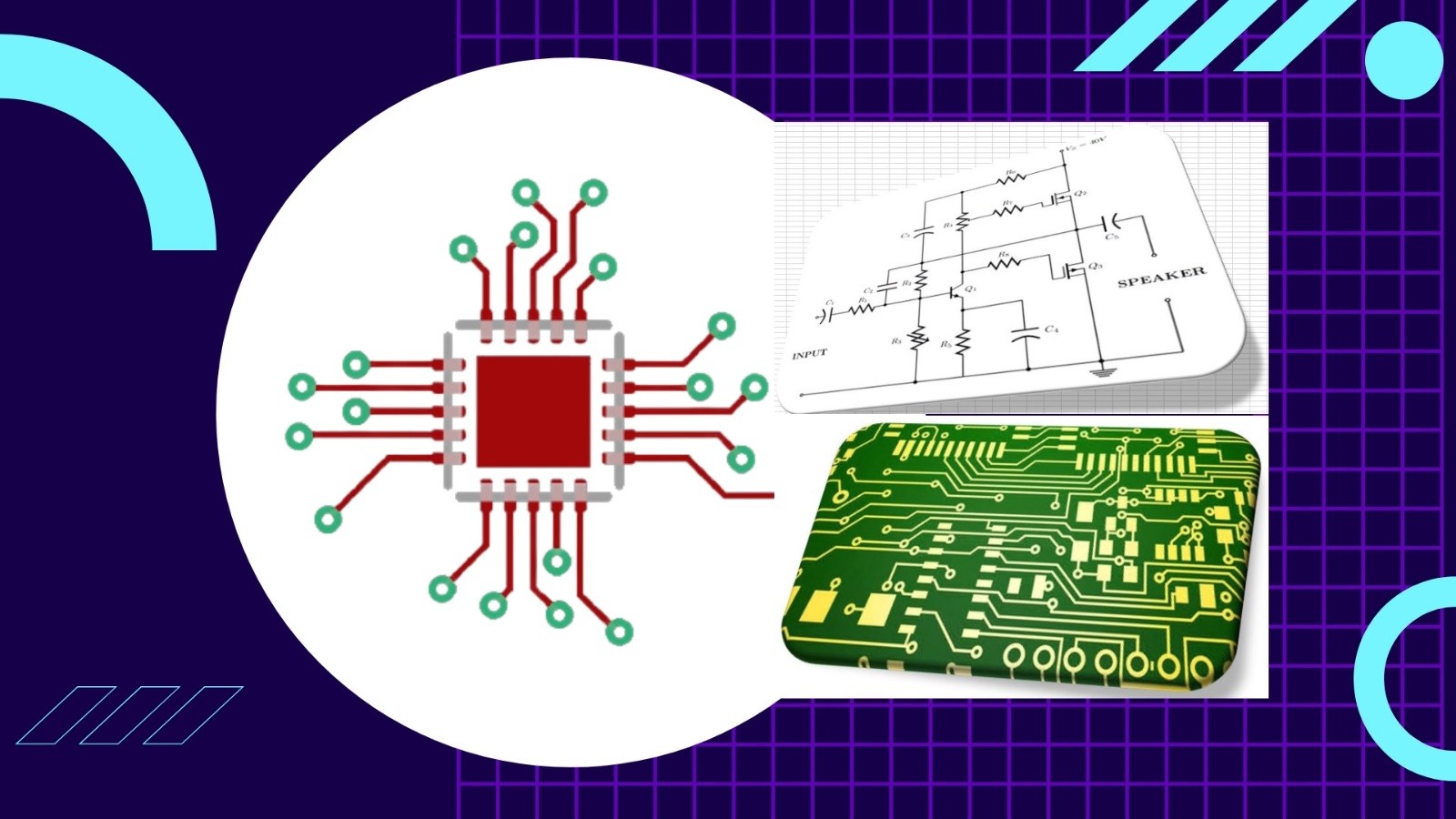
PCB Design and electronics circuit are basements for all type of electronics products. PCBs are derived from the analog and digital circuits which are prepared according to the application required. Printed circuit boards are the main pillars of the Electronics world. Every Electronics products has PCB inside it, from consumer gadgets like computers, smart phones and gaming consoles to industry and even high-tech products.
Required eligibility:
Diploma in Electrical or Electronics & Communication.
BE/BTech. in Electrical or Electronics & Communication.
BSc/MSc in Electronics & Communication.
ME/MTech. (E&CE) in Communication.
PCB Design Course Content is given below in brief:
Schematic Design:
Basic Electronics theory.
Basics of Circuit designing.
Schematic design preparation.
Schematic part editing and creation.
Net list and Net class creation.
Bill Of Material generation (BOM).
Electrical Rule Checking.
Footprint Creation:
Through hole footprint creation.
Surface Mount Device footprint creation.
BGA/PGA footprint creation.
Board Designing:
Board size and shape creation.
Component placements.
PCB Routing: 2 to 16 Layer routing.
Plane creation.
Design rule checking.
Gerber generation.
Skills you gain after the course completion:
Basic Electronics and Electronic components expertise.
Circuit Designing (Power management circuit designing)
Circuit Simulation for best understanding of the subject.
Tools/Software Expertise.
Basic design module practice up to 4-Layers.
Advanced design module practice up to 16-Layers.
Design expertise:
o Assignments consists single and double sided PCB.
o Assignments consists 2-Layers to 16-Layers design.
Library Module:
o Symbol and Footprint design for all types of packages.
High speed placements & routing techniques.
Power integrity and Signal Integrity analysis.
Design for Manufacturing, Testing and Fabrication expertise.
Gerber generation and editing.
COURSE CONTENT
35 Lessons 09:37:35
Lesson- 1: Introduction to Course: What we will learn? Preview 00:05:15
Lesson- 2: Introduction to Eagle CAD Environment 00:31:20
Lesson- 3: Circuit design Simulation and Analysis 00:18:29
Lesson- 1: An Introduction: Working with Library Symbol Creation Preview 00:23:20
Lesson- 2: Symbol Creation: Resistor 00:19:41
Lesson- 3: Symbol Creation: Capacitor 00:25:56
Lesson- 4: Symbol Creation: Inductor 00:16:53
Lesson- 5: Symbol Creation: Transformer 00:22:44
Lesson- 6: Symbol Creation: Diode 00:22:59
Lesson- 7: Symbol Creation: Transistor 00:16:38
Lesson- 8: Symbol Creation: Logic Gates 00:15:31
Lesson- 9: Symbol Creation: Connectors 00:16:47
Lesson- 10: Symbol Creation: Integrated Circuits (ICs) 00:28:57
Lesson- 11: Symbol Creation: Miscellaneous 00:16:51
Lesson- 1: Footprint Creation: Resistor (Surface mount package) 00:24:06
Lesson- 2: Footprint Creation: Resistor (Through hole package) 00:15:10
Lesson- 3: Footprint Creation: Capacitor (Surface Mount Package) 00:10:36
Lesson- 4: Footprint Creation: Capacitor (Through Hole Package) 00:08:18
Lesson- 5: Footprint Creation: Connector (Through Hole Packages) 00:10:39
Lesson- 6: Footprint Creation: Connector (Surface Mount Device Package) 00:08:35
Lesson- 7: Footprint Creation: ICs (Surface Mount Device Packages) 00:11:18
Lesson- 8: Footprint Creation: ICs (Through Hole Packages) 00:09:32
Lesson- 9: Assignments of Footprint Development. 00:07:19
Lesson- 1: Introduction: Setting up Grids and User Interface 00:10:30
Lesson- 2: Circuit Preparation in Schematic level 00:55:08
Lesson- 3: Electrical Rule Checking and Net naming 00:11:28
Lesson- 4: Exporting Schematic Files 00:10:20
Lesson- 5: Schematic Preparations: Assignments 00:03:52
Lesson- 1: Switching to Board: An Introduction to Board Design Environment 00:06:21
Lesson- 2: Board Shape Creation 00:12:07
Lesson- 3: Constraints Settings: DRC entry, Net class and Rules 00:19:32
Lesson- 4: Component Placements: Top and Bottom sides 00:21:17
Lesson- 5: PCB Routing: Complete Guidelines 00:26:29
Lesson- 6: Copper Plan Creation 00:03:45
Lesson- 7: Gerber Generation 00:09:52
SIMILAR COURSES
COURSE FEATURES
35 Lessons
Full Lifetime Access
Access on Mobile
Access on Web
Certificate of Completion
Full Lifetime Access
Access on Mobile
Access on Web
Certificate of Completion
M.R.P.:
₹ 1499.00
ISC Price:₹ 999.00
You Save: ₹ 500 (33.36% off)
ISC Price:
You Save: ₹ 500 (33.36% off)
DON'T HAVE TIME?
We can send you everything you need to know about this course through email.
We respect your privacy. your information is safe and will never be shared.
